Şimdi Ara

e8500 + apogee gtz + koolance exos + dfi x48

Daha Fazla
Bu Konudaki Kullanıcılar: Daha Az
1 Misafir - 1 Masaüstü
5 sn
5
Cevap
0
Favori
1.948
Tıklama
Daha Fazla
İstatistik
  • Konu İstatistikleri Yükleniyor
0 oy
Öne Çıkar
Sayfa: 1
Giriş
Mesaj
  • bu işlemci artık son demlerinde ama hala overclock denemekten sıkılmadım. herhalde intelin parasını hakeden nadir işlemcilerinden birisir.
    dfi p45 anakartım bozulunca x48 le degiştirdim. daha once 4390 da tıkanan işlemci x48 le rahat 9 x 500 calisiyor. voltajı biraz daha gıdıklasam rahat gunluk 4700 mhz calisir.
    su anda gunluk 9 x 500 calisyor (1.34 V). yuk altında sıcaklık degerleri 57-58 derece civarı. benchlerin hepsini 4500 mhz de aldım. orthos ve futuremakrlar bucuklu carpanıda goruyor. o yuzden 4750 mhz gozukuyor.

     e8500 + apogee gtz + koolance exos + dfi x48

     e8500 + apogee gtz + koolance exos + dfi x48

     e8500 + apogee gtz + koolance exos + dfi x48

     e8500 + apogee gtz + koolance exos + dfi x48

     e8500 + apogee gtz + koolance exos + dfi x48


    ilgilenenler için bios ayarlarım
    Genie BIOS Setting

    Exit Setup shutdown........................... - Mode 2
    O.C. Fail retry Counter....................... - 1
    O.C. Fail CMOS Reload......................... - Disabled
    CPU Clock Ratio............................... - 9X
    CPU N/2 Ratio................................. - Disabled
    Target CPU Clock.............................. - 4500 MHz
    CPU Clock..................................... - 500 MHz
    Boot Up Clock................................. - Auto
    CPU Clock Amplitude........................... - 800mV
    CPU Clock0 Skew............................... - 200ps
    CPU Clock1 Skew............................... - 0ps
    DRAM Speed.................................... - 333/667
    Target DRAM Speed............................. - DDR2 1001
    PCIE Clock.................................... - 100 MHz

    CPU Spread Spectrum........................... - Disabled
    PCIE Spread Spectrum.......................... - Disabled


    CPU Feature

    Thermal Management Control.................... - Enabled
    PPM (EIST)Mode................................ - Disable
    Limit CPUID MaxVal............................ - Disabled
    C1E Function.................................. - Disable
    Execute Disable Bit........................... - Disable
    Virtualization Technology..................... - Disable
    Core Multi-Processing......................... - Enabled


    DRAM Timing

    Enhance Data Transmitting..................... - Fast
    Enhanced Addressing........................... -Fast
    T2 Dispatch................................... - Auto

    Flex Memory Mode.............................. - Auto
    CAS Latency Time (tCL)........................ - 5
    RAS# to CAS# Delay (tRCD)..................... - 5
    RAS# Precharge (tRP).......................... - 5
    Precharge Delay (tRAS)........................ - 15
    All Precharge to ACT.......................... - 5
    REF to ACT Delay (tRFC)....................... -48
    Performance LVL (Read Delay).................. 9
    Write to PRE Delay (tWR)...................... - 14
    Rank Write to Read (tWTR)..................... - 11
    ACT to ACT Delay (tRRD)....................... -3
    Read to Write Delay (tRDWR)................... - 8
    Ranks Write to Write (tWRWR).................. - Auto
    Ranks Write to Read (tWRRD)................... -Auto
    Read CAS# Precharge (tRTP).................... - 3
    All PRE to Refresh............................ - 3


    Clock Setting Fine Delay

    DRAM Clock Driving Strength........................ - Level 6
    DRAM Data Driving Strength......................... - Level 8
    Ch1 DLL Default Skew Model......................... - 3
    Ch2 DLL Default Skew Model..........................- 3

    Fine Delay Step Degree........................ - 75ps

    Ch1 Clock Crossing Setting.................... - Auto
    DIMM 1 Clock fine delay....................... - current 2149ps
    DIMM 2 Clock fine delay....................... - current 362ps
    DIMM 2 Control fine delay..................... - current 1100ps
    DIMM 1 Control fine delay..................... - current 1037ps
    Ch1 Command fine delay........................ - current 1100ps

    Ch2 Clock Crossing Setting.................... - Auto
    DIMM 3 Clock fine delay....................... - current 2162ps
    DIMM 4 Clock fine delay....................... - current 362ps
    DIMM 4 Control fine delay..................... - current 1162ps
    DIMM 3 Control fine delay..................... - current 1112ps
    Ch1 Command fine delay........................ - current 1162ps

    Ch1Ch2 Common Clock Setting................... - Auto

    Ch1 RDCAS GNT-Chip Delay...................... - Auto
    Ch1 WRCAS GNT-Chip Delay...................... - Auto
    Ch1 Command to CS Delay....................... - Auto

    Ch2 RDCAS GNT-Chip Delay...................... - Auto
    Ch2 WRCAS GNT-Chip Delay...................... - Auto
    Ch2 Command to CS Delay....................... - Auto


    Voltage Setting

    CPU VID Control.............................. - 1.22500V
    CPU VID Special Add...........................- 115%
    DRAM Voltage Control.......................... - 2.125V
    SB Core/CPU PLL Voltage....................... - 1.640V
    NB Core Voltage............................... - 1.317V
    CPU VTT Voltage............................... - 1.134V
    Vcore Droop Control........................... - Disabled
    Clockgen Voltage Control...................... - 3.60V
    GTL+ Buffers Strength......................... - Strong
    Host Slew Rate................................ - Weak
    MCH RON Offset Value.......................... - 00
    MCH RTT Offset Value.......................... - 00
    MCH VREF 1 Value.............................. - 00
    MCH VREF 2 Value.............................. - 00
    MCH VREF 3 Value.............................. - 00
    CPU GTL 0/2 REF Volt.......................... - 0.667X
    CPU GTL 1/3 REF Volt.......................... - 0.667X
    North Bridge GTL REF Volt..................... - 0.61X
    FSB Vref...................................... - 2A


  • Gerçekten iyi iş çıkartmışsın
    Soğutu olarak ne kullandın acaba? Birde işlemcinin VID değeri nedir ?


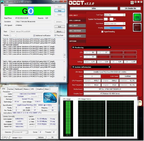
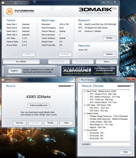
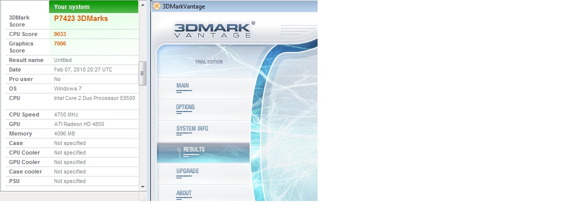
    < Bu mesaj bu kişi tarafından değiştirildi schurzenjager -- 8 Mart 2010; 13:45:50 >
  • quote:

    Orijinalden alıntı: mk2kill

    bu işlemci artık son demlerinde ama hala overclock denemekten sıkılmadım. herhalde intelin parasını hakeden nadir işlemcilerinden birisir.
    dfi p45 anakartım bozulunca x48 le degiştirdim. daha once 4390 da tıkanan işlemci x48 le rahat 9 x 500 calisiyor. voltajı biraz daha gıdıklasam rahat gunluk 4700 mhz calisir.
    su anda gunluk 9 x 500 calisyor (1.34 V). yuk altında sıcaklık degerleri 57-58 derece civarı. benchlerin hepsini 4500 mhz de aldım. orthos ve futuremakrlar bucuklu carpanıda goruyor. o yuzden 4750 mhz gozukuyor.

     e8500 + apogee gtz + koolance exos + dfi x48

     e8500 + apogee gtz + koolance exos + dfi x48

     e8500 + apogee gtz + koolance exos + dfi x48

     e8500 + apogee gtz + koolance exos + dfi x48

     e8500 + apogee gtz + koolance exos + dfi x48


    ilgilenenler için bios ayarlarım
    Genie BIOS Setting

    Exit Setup shutdown........................... - Mode 2
    O.C. Fail retry Counter....................... - 1
    O.C. Fail CMOS Reload......................... - Disabled
    CPU Clock Ratio............................... - 9X
    CPU N/2 Ratio................................. - Disabled
    Target CPU Clock.............................. - 4500 MHz
    CPU Clock..................................... - 500 MHz
    Boot Up Clock................................. - Auto
    CPU Clock Amplitude........................... - 800mV
    CPU Clock0 Skew............................... - 200ps
    CPU Clock1 Skew............................... - 0ps
    DRAM Speed.................................... - 333/667
    Target DRAM Speed............................. - DDR2 1001
    PCIE Clock.................................... - 100 MHz

    CPU Spread Spectrum........................... - Disabled
    PCIE Spread Spectrum.......................... - Disabled


    CPU Feature

    Thermal Management Control.................... - Enabled
    PPM (EIST)Mode................................ - Disable
    Limit CPUID MaxVal............................ - Disabled
    C1E Function.................................. - Disable
    Execute Disable Bit........................... - Disable
    Virtualization Technology..................... - Disable
    Core Multi-Processing......................... - Enabled


    DRAM Timing

    Enhance Data Transmitting..................... - Fast
    Enhanced Addressing........................... -Fast
    T2 Dispatch................................... - Auto

    Flex Memory Mode.............................. - Auto
    CAS Latency Time (tCL)........................ - 5
    RAS# to CAS# Delay (tRCD)..................... - 5
    RAS# Precharge (tRP).......................... - 5
    Precharge Delay (tRAS)........................ - 15
    All Precharge to ACT.......................... - 5
    REF to ACT Delay (tRFC)....................... -48
    Performance LVL (Read Delay).................. 9
    Write to PRE Delay (tWR)...................... - 14
    Rank Write to Read (tWTR)..................... - 11
    ACT to ACT Delay (tRRD)....................... -3
    Read to Write Delay (tRDWR)................... - 8
    Ranks Write to Write (tWRWR).................. - Auto
    Ranks Write to Read (tWRRD)................... -Auto
    Read CAS# Precharge (tRTP).................... - 3
    All PRE to Refresh............................ - 3


    Clock Setting Fine Delay

    DRAM Clock Driving Strength........................ - Level 6
    DRAM Data Driving Strength......................... - Level 8
    Ch1 DLL Default Skew Model......................... - 3
    Ch2 DLL Default Skew Model..........................- 3

    Fine Delay Step Degree........................ - 75ps

    Ch1 Clock Crossing Setting.................... - Auto
    DIMM 1 Clock fine delay....................... - current 2149ps
    DIMM 2 Clock fine delay....................... - current 362ps
    DIMM 2 Control fine delay..................... - current 1100ps
    DIMM 1 Control fine delay..................... - current 1037ps
    Ch1 Command fine delay........................ - current 1100ps

    Ch2 Clock Crossing Setting.................... - Auto
    DIMM 3 Clock fine delay....................... - current 2162ps
    DIMM 4 Clock fine delay....................... - current 362ps
    DIMM 4 Control fine delay..................... - current 1162ps
    DIMM 3 Control fine delay..................... - current 1112ps
    Ch1 Command fine delay........................ - current 1162ps

    Ch1Ch2 Common Clock Setting................... - Auto

    Ch1 RDCAS GNT-Chip Delay...................... - Auto
    Ch1 WRCAS GNT-Chip Delay...................... - Auto
    Ch1 Command to CS Delay....................... - Auto

    Ch2 RDCAS GNT-Chip Delay...................... - Auto
    Ch2 WRCAS GNT-Chip Delay...................... - Auto
    Ch2 Command to CS Delay....................... - Auto


    Voltage Setting

    CPU VID Control.............................. - 1.22500V
    CPU VID Special Add...........................- 115%
    DRAM Voltage Control.......................... - 2.125V
    SB Core/CPU PLL Voltage....................... - 1.640V
    NB Core Voltage............................... - 1.317V
    CPU VTT Voltage............................... - 1.134V
    Vcore Droop Control........................... - Disabled
    Clockgen Voltage Control...................... - 3.60V
    GTL+ Buffers Strength......................... - Strong
    Host Slew Rate................................ - Weak
    MCH RON Offset Value.......................... - 00
    MCH RTT Offset Value.......................... - 00
    MCH VREF 1 Value.............................. - 00
    MCH VREF 2 Value.............................. - 00
    MCH VREF 3 Value.............................. - 00
    CPU GTL 0/2 REF Volt.......................... - 0.667X
    CPU GTL 1/3 REF Volt.......................... - 0.667X
    North Bridge GTL REF Volt..................... - 0.61X
    FSB Vref...................................... - 2A

    hocam aynı anakart ve aynı işlemcide bende var oc konusunda acil yardımına ihtiyacım var pek oc bilmiyorum lütfen bana bir ulas :/ 0506 673 78 82


  • SM 2 we SM 3 skorlari, benim eski overclock'lu 8800GT hava sogutma ile neredeyse ayni sayilir (+ islemci de default halde iken).
  • 
Sayfa: 1
- x
Bildirim
mesajınız kopyalandı (ctrl+v) yapıştırmak istediğiniz yere yapıştırabilirsiniz.